 |
Serial sequential adder
v.1.0
Example documentation project, author Vladimir Petrović
|
 |
Serial sequential adder
v.1.0
Example documentation project, author Vladimir Petrović
|
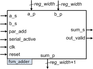
The fsm_adder is a sequential component that can serially add two binary numbers of any length. It has two input shift registers of width defined in generic reg_width and one output shift register of width reg_width+1 since the addition result is one bit longer than the addends. The interface description is shown in Fig. 1.

The component can work in two modes:
The timing diagram of serial addition of two 4 bit numbers in mode 1 (parallel load) is shown in Fig.2. After the paralel load of input numbers, the fsm_adder needs 4+1=5 clk periods to calculate the result. When the sum is ready it is valid at the sum_p output and fsm_adder generates the logical 1 at out_valid output.

The timing diagram of serial addition of two 6 bit numbers (a = 100101, b = 011110) in mode 2 (serial load) is shown in Fig.3. Firstly, the serial_active signal is set to 1. fsm_adder needs one clk cycle to start sampling the serial inputs a_s and b_s. After 1+4+5=9 clk cycles from the moment when serial_active was first set to 1, first bit of the result can be sampled form sum_s output. out_valid is active as long as the output sum bits are valid. In this example, the output is 7-bit long number 1000011, or in decimal representation: a+b=37+30=67. When the sum is ready it is valid at the sum_p output and fsm_adder generates the logical 1 at out_valid output.

This project is done for the need of the Technical documentation course at the Department of Electronics, School of Electrical Engineering. Some code needs more comments and/or doxygen oriented comments for better documentation output.
Here we should describe the structure of the documentation, but it is 2:33 AM and we move the description to the TODO list. :)
Anyone can use these documents for non-commercial use without any restrictions.
 1.8.12